By 13001 Transistor 1806
Technical Parameters and Performance
Real Applications and Circuit Design
How to Use the 13001 Transistor
13001 is a common NPN silicon high-frequency and high-voltage Bipolar Junction Transistor (BJT). It is mainly used in switching applications of Switch Mode Power Supply (SMPS), especially in low-power systems.
The 13001 transistor uses a standard NPN structure. Two N-type semiconductor layers are on both sides of a P-type semiconductor layer.
This structure forms three terminals: emitter, base, and collector.
When the base-emitter junction is forward-biased, electrons move from the emitter to the base, and then the collector collects them. This controls the collector current.
This structure gives the device high voltage capability and fast switching speed.
The 13001 transistor has different package types for different needs:
Compared with other transistors, the package design of the 13001 focuses on cost optimization. For example, the thermal resistance of the TO-92 package is about 200°C/W. Similar products often have 150-200°C/W. This shows a balance of cost and performance.
The 13001 transistor has these features:
The key ratings define the safe working area:
| Parameter | Symbol | Value | Condition |
| Collector-Emitter Voltage | Vceo | 400V | Ic = 1mA |
| Collector-Base Voltage | Vcbo | 500V | Ic = 100μA |
| Emitter-Base Voltage | Vebo | 6V | Ie = 100μA |
| Collector Current | Ic | 300mA | – |
| Power Dissipation | Pc | 0.75W | Ta = 25°C |
| Junction Temperature | Tj | 150°C | – |
| Storage Temperature | Tstg | -55~150°C | – |
The Vceo of 13001 reaches 400V. Normal low-cost transistors usually only have 250–300V. This gives the 13001 better reliability in high-voltage use.
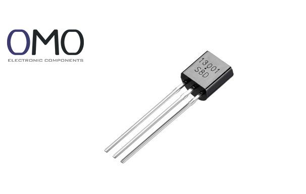
TO-92 is the most common package.
With the flat side facing you and pins pointing downward, the pin order is:
This is similar to many general transistors. You can use a multimeter to confirm the pins.
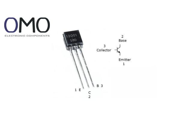
Important: Different manufacturers may use different pin orders. Always check the datasheet to avoid damage.
The 13001 transistor is widely used in
The 13001 can be used to drive loads with a microcontroller.
Collector → load → power.
Emitter → ground.
Base → control signal through a resistor.
When the control signal is HIGH, the transistor turns on and the load works.
Base resistor formula:
Rb = (Vdrive - Vbe) / Ib
Where: Vbe ≈ 0.7V, Ib is usually 1/10–1/20 of Ic.
In a Flyback Converter (flyback topology), the 13001 works as a switching transistor.
Its high voltage rating allows it to handle voltage spikes.
Its fast switching reduces loss and improves efficiency.
Compared with older BJTs, losses can be reduced by about 30%.
Limited frequency: Not as good as MOSFET in high-frequency use
| Model | Vceo | Ic | Package | Feature |
| 13002 | 400V | 0.6A | TO-92 | Higher current |
| 13003 | 400V | 1.5A | TO-126 | Higher power |
| 2SC2611 | 400V | 0.1A | TO-92 | Similar parameters |
| MPSA42 | 300V | 0.5A | TO-92 | Lower voltage |
| KSP92 | 400V | 0.5A | TO-92 | Direct replacement |
Check these when choosing a replacement:
13001 has the best balance of cost and performance.
Its price is only 60-80% of other models.
Formula: Rb ≤ (Vdrive - Vbe) / (Ic / hFE_min)
Power loss formula: Pdiss = Vce × Ic
Pdiss must be lower than Pc_max
BE and BC forward voltage ≈ 0.6-0.7V, reverse = open;
CE should be high resistance both ways.
A 13001 transistor is an NPN-type silicon power transistor frequently employed in switching applications. Typical uses include electronic ballasts for energy-efficient lighting, battery chargers, and switch-mode power supply units. This component is recognized for its capacity to support comparatively high voltage and current levels.
Bipolar transistors function as fundamental components for amplifying or switching electronic signals. Their applications range from acting as switches in digital circuits and amplifiers in analog designs to uses in voltage regulation, oscillator generation, and signal modulation.
The 13001 is an NPN transistor designed for high-voltage, low-power switching applications. Common substitutes or equivalent models include other transistors from the 1300X series, such as the 13002, 13003, 13005A, and 13009, as well as the APT13005D and MJE13007.
The 13001 is an NPN Bipolar Junction Transistor (BJT). In this NPN type, applying a positive bias to the base allows current to flow from the collector to the emitter.