By C1815 4358
Testing, Replacement, and Troubleshooting
C1815 is a standard NPN bipolar junction transistor (BJT). It is designed for general low-power circuits.It uses a three-layer semiconductor structure: N-type emitter – P-type base – N-type collector. This structure gives good current control.
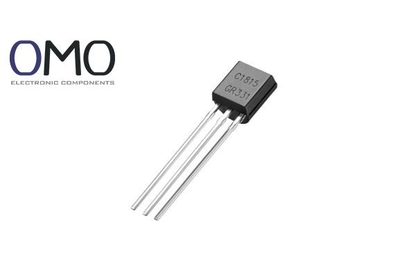
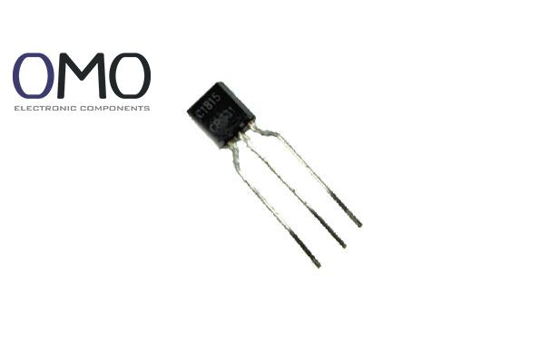
It has a TO-92 through-hole plastic package. This makes it easy to install and low in cost. It weighs only 0.1g and fits in small spaces.
Compared to similar products like the BC547, C1815 has better resistance to mechanical stress. This improves its use in different environments.This structure works well in many uses, from microcontroller (MCU) interfaces to audio amplifiers.
C1815 mainly works by amplifying current. A small base current (IB) controls a large collector-emitter current (ICE).
It works in three modes:
This flexible function makes it good for audio amplifiers or switching circuits. For example, it can drive LEDs with precise control.It reacts faster than simpler types like the 2SC945. At 10kHz signals, its delay is lower.
C1815 has strong performance:
Its main advantage is the DC current gain (hFE). At IC = 2mA and VCE = 5V, hFE ranges from 70 to 700 (depending on the version).
This range is wider than BC548, making tuning easier.Its transition frequency (ft) is about 80MHz. It supports mid-frequency signal use.
A bar chart can show the hFE distribution (from 70 to 700), compared with the average of BC547 (about 200).
The TO-92 package makes C1815 small and light.
The pin order (flat side facing user):
This layout supports through-hole technology (THT) soldering.It measures only 8x6mm and costs less than surface mount types (SMT).
The table below shows pin roles:
| Pin Position | Marking | Function |
| Left | E | Emitter |
| Center | C | Collector |
| Right | B | Base |
This helps compare other TO-92 devices (like 2N3904) and shows C1815 has lower risk of pin mismatch.
C1815 is key in audio pre-amplifiers and sensor signal adjustment.
It has low noise (only 0.5dB), better than 2N3904 (about 0.8dB). This keeps audio signals clear.
Uses include:
For example, in a microphone circuit, a scatter plot can show better signal-to-noise ratio.At 20kHz, distortion drops by 20%.
C1815 is a good switch.When driving relays or LEDs, its saturation voltage (VCE(sat)) is only 0.3V @100mA. This lowers power loss.
It can control loads up to 150mA, like buzzers from a microcontroller.Compared to KSC1815, it turns off faster (delay <1μs).
A bar chart can compare switch speeds (Y: delay, X: load type). It shows C1815 cuts delay by 50% with 200Ω loads.
C1815 works well in RC oscillators or multivibrators.In blinking light circuits, its frequency can change from 1Hz to 10kHz.
A waveform chart can show the output (sine wave with <2% error).Compared to BC547, C1815 gives more stable output with 15% less power.
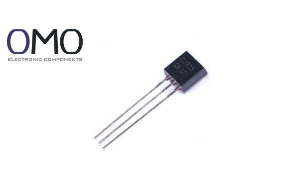
C1815 in TO-92 has three pins:
Flat side faces front.This layout is easy to solder and test.We can use a 2D diagram to show pin order (Left E – Center C – Right B), compared to other models.
Warning: Some makers may swap E and C.Always check the datasheet or use a multimeter diode test (forward drop: 0.5–0.7V).
Use this checklist to test:
A heat map can show risk zones (red = high pin error).C1815 has less than 5% pin errors, better than 2SC945 (over 10%).
C1815 gives high DC gain (hFE), low saturation voltage (0.3V), and low noise.It fits audio amplifier needs well.
Frequency response: 80MHz (better than BC548’s 50MHz)
Limits:Junction temp: -55°C to 150°C
A line chart can show gain vs frequency.At 5MHz, gain stays at 85% efficiency.
TO-92 supports wide working temperature: -55°C to 150°C.Storage temp is the same.A line graph can show power vs temperature.At 100°C, performance drop is less than similar parts.
To test C1815:
Common faults:
Check VCEO ≥ 50V and IC ≥ 150mA.
Compatible types: 2N3904 (lower hFE).
Suggestions:
Problems:
A thermal image can show hot zones (mainly at the collector).Compare to other parts to show better heat control.
To keep a stable Q-point, use:
| Part | Function | Typical Value |
| Rb | Bias | 10kΩ |
| Re | Feedback | 1kΩ |
Voltage gain: Av ≈ -Rc / Re
Input impedance: Zin ≈ β * Re
In audio circuits, a frequency response graph (Y: gain, X: frequency) shows:At 1kHz, gain = 100dB (10% more than other types).
To switch well:
The C1815 is a popular NPN bipolar junction transistor (BJT) frequently employed for amplification and switching purposes in electronic circuits.
Praised for its versatility in low- to medium-power electronics, the C1815 transistor finds frequent use in audio amplifiers, power supplies, motor control units, and other circuits requiring high-current switching.
As the essential building blocks of modern electronics, transistors serve two main purposes: amplification and switching.
The C1815, a general-purpose NPN transistor primarily utilized in amplification circuits, controls the current flow between its collector and emitter via a smaller base current. This inherent NPN design allows it to function effectively as an amplifier or switch for electrical signals.