By Texas Instruments 1571
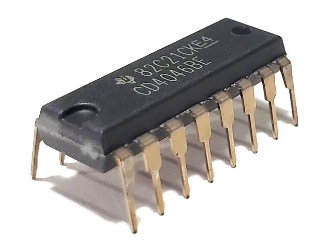
CD4046BE is a CMOS integrated circuit. It is a phase locked loop (PLL) circuit used in applications such as frequency synthesis and clock recovery. PLL is an electronic circuit that compares the phase of the input signal with a local reference signal, and then synchronizes the input signal with the reference signal by adjusting the frequency of the VCO (Voltage-Controlled Oscillator, Voltage Controlled Oscillator).

Ⅰ.Specifications of CD4046BE
•Type:PLL
•Technology:Si
•Number of pins:16
•Output level:CMOS
•Number of circuits:1 Circuit
•Supply voltage-Minimum:3 V
•Supply voltage-Maximum:18 V
•Product Category:Phase Locked Loop-PLL
•Height:4.57 mm
•Length:19.3 mm
•Width:6.35 mm
•Minimum operating temperature:-55℃
•Maximum operating temperature:+125℃
•Maximum input frequency:2.4 MHz
•Minimum input frequency:300 kHz
•Number of output interfaces:1
•Contact plating:gold
•Power supply voltage:10V
•Radiation Hardening:No
•Supply current:10 mAv
•ECCN code:EAR99
•Terminal location:Dual
•Package/Case:PDIP-16
•Installation style:Through Hole
•Operating power supply voltage:3 V to 18 V
•Input:Complementary Metal Oxide Semiconductors
•RoHS status:complies with ROHS3 standards
•REACH SVHC standard:No SVHC
•Moisture Sensitivity Level (MSL):1 (no limit)
•Output frequency range:300 kHz to 2.4 MHz
•Product type:PLLs-Phase Locked Loops
Ⅱ.Main uses of CD4046BE
1.Frequency capture: When the frequency of the input signal changes, CD4046BE can automatically track and adjust the frequency of the VCO to achieve frequency capture.
2.Frequency synthesis: CD4046BE is indeed used to generate a stable output frequency related to the input frequency to achieve frequency synthesis. This is usually accomplished through microprocessor control, by adjusting the frequency of the VCO (Voltage Controlled Oscillator) so that it is synchronized with the input signal.
3.Frequency modulation: CD4046BE can be used to implement frequency modulation, modulating the frequency of an analog signal to a specific range.
4.Clock recovery: In digital communication and data transmission, CD4046BE can be used for clock recovery to ensure that the receiving end can correctly parse the clock information of the input data stream.
5.FM Demodulator: CD4046BE can be used as part of an FM demodulator to modulate and demodulate frequencies in wireless communications. Its frequency synthesis and frequency acquisition functions enable it to be used to implement signal modulation and demodulation in wireless communications to achieve data transmission and reception.
6.Clock generation: In digital systems, CD4046BE can be used to generate stable clock signals to ensure the synchronous operation of all parts of the system. The frequency synthesis function of CD4046BE enables it to generate high-precision and high-stability clock signals to meet the needs of various digital systems.
Ⅲ.Application fields of CD4046BE
•Audio equipment
•Radio
•Communication Systems
•Digital system clock generation
•Data transmission
•Radar system
•Instrument measuring equipment
•Remote sensing system
•Frequency capture
•Frequency modulation and demodulation
•FSK-Modems
•Signal conditioning
•Tone decoding
•Date synchronization
•Voltage-to-frequency conversion
Ⅳ.Working principle of CD4046BE
1.Phase comparator: The phase comparator of CD4046BE receives the input signal (reference signal) and the VCO output signal, and compares their phase difference. If the phase of the VCO output signal lags behind the reference signal, the phase comparator will generate a positive voltage, causing the VCO frequency to increase; if the phase of the VCO output signal leads the reference signal, the phase comparator will generate a negative voltage, causing the VCO frequency to increase. decrease. In this way, CD4046BE automatically adjusts the frequency of the VCO to keep the phase of the VCO output signal synchronized with the reference signal.
2.VCO (Voltage-Controlled Oscillator): VCO is an oscillator whose output frequency is affected by the control voltage. CD4046BE attempts to minimize the phase difference between the input signal and the VCO output signal by adjusting the frequency of the VCO, thereby achieving phase locking.
3.Loop Filter: The phase difference signal passes through the loop filter, which is used to filter out high-frequency noise and generate a control voltage. This control voltage will affect the frequency of the VCO.
4.Feedback loop: The output signal of the VCO returns to the phase comparator through the feedback loop and is compared with the input signal in phase. By continuously adjusting the frequency of the VCO, the phase difference is as close to zero as possible, thereby achieving phase locking.
5.Control voltage adjustment: The control voltage generated by the loop filter is adjusted according to the direction and amplitude of the phase difference signal to guide the frequency of the VCO in a direction that matches the input signal.
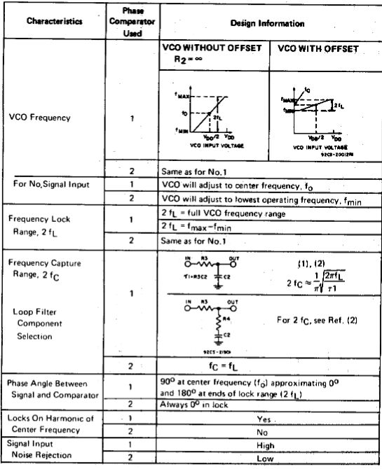
Ⅴ.Design Information of CD4046BE

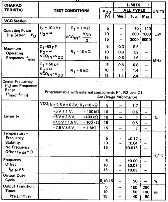
Ⅵ.Electrical Characteristics at TA=25℃ of CD4046BE

Ⅶ.Circuit connection method of CD4046BE
1.Power supply: CD4046BE requires a stable DC power supply. An appropriate power management chip or voltage regulator is usually used to provide the required supply voltage.
2.Input signal: The input signal of CD4046BE is usually a stable reference frequency source, which can be a quartz crystal oscillator, ceramic resonator or other frequency-stable signal source. The input signal is connected to the input of the phase comparator.
3.VCO (voltage controlled oscillator): VCO is one of the core components of CD4046BE, and the frequency of its output signal is affected by the control voltage. The output signal of the VCO is connected to the other input of the phase comparator.
4.Phase comparator: The phase comparator receives the input signal and the VCO output signal and compares their phase difference. The phase comparator generates a phase difference signal, which controls the frequency adjustment of the VCO.
5.Other components: Depending on the actual application requirements, it may be necessary to add some other components, such as resistors, capacitors, etc., to achieve specific functions or improve the performance of the circuit.
Ⅷ.How does CD4046BE realize the function of frequency locked loop (PLL)?
1.Input signal phase comparison: The phase comparator input pin of CD4046BE (usually pin 3, phase comparator input-INPHASE) receives the input signal, that is, the reference signal or reference frequency. The phase comparator may also receive a signal that is 90 degrees out of phase (usually pin 14, phase comparator input - QUADRATURE).
2.Phase difference signal generation: The phase comparator compares the phase of the input signal and the VCO output signal to generate a phase difference signal. This phase difference signal represents the phase difference between the input signal and the VCO output signal.
3.VCO frequency adjustment: The control voltage enters the VCO control voltage input pin (usually pin 6, VCO control voltage input-VCO IN). The VCO adjusts its own oscillation frequency according to the control voltage.
4.Loop filter processing: The phase difference signal enters the loop filter, which is used to filter out high-frequency noise and generate a control voltage. This control voltage will affect the frequency of the VCO.
5.Feedback loop: The output signal of the VCO returns to the phase comparator through pin 4 (negative feedback input-COMP IN) for phase comparison with the input signal. By continuously adjusting the frequency of the VCO, the phase difference is as close to zero as possible, thereby achieving phase locking.
Ⅸ.Alternate model of CD4046BE
•CD4046BE
•CD4046BEE4
•CD74HC4046AE
•CD74HCT4046AE
Frequently Asked Questions
1.What are the features of CD4046BE?
It has the characteristics of low power consumption, phase comparator, linear voltage controlled oscillator standardization, and symmetrical output.
2.What is CD4046BE?
CD4046BE is a CMOS phase-locked loop (PLL) integrated circuit. It is commonly used for frequency synthesis and clock recovery applications.
3.How does CD4046BE handle frequency capture in the presence of input signal variations?
CD4046BE has a fast frequency capture capability, allowing it to quickly track changes in the input signal frequency and adjust the VCO's frequency to maintain phase lock.
4.How can stability issues in the output waveform of CD4046BE be addressed?
Stability issues in the output waveform can be addressed by checking the VCO power supply, ensuring proper control voltage, and reviewing the components in the loop filter.