By Analog Devices Inc 916
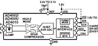
ADI’s AD4002/AD4006/AD4010 are low noise, low power, high speed, 18-bit, precision successive approximation register (SAR) analog-to-digital converters (ADCs). The throughput for the AD4002 is 2 MSPS, for the AD4006 it is 1 MSPS, and for the AD4010 it is 500 kSPS. These devices incorporate ease of use features that lower the signal chain power, reduce signal chain complexity, and enable higher channel density. The high-Z mode, coupled with a long acquisition phase, eliminates the need for a dedicated high power, high-speed ADC driver, thus broadening the range of low power precision amplifiers that can drive this ADC directly while still achieving optimum performance. The input span compression feature enables the ADC driver amplifier and the ADC to operate off common supply rails without the need for a negative supply while preserving the full ADC code range. The low serial peripheral interface (SPI) clock rate requirement reduces the digital input/output power consumption, broadens processor options, and simplifies the task of sending data across digital isolation.
Operating from a 1.8 V supply, the an analog input (IN+) between 0 V to VREF with respect to a ground sense (IN−) with VREF ranging from 2.4 V to 5.1 V. The SPI-compatible versatile serial interface features seven different modes including the ability, using the SDI input, to daisy-chain several ADCs on a single 3-wire bus and provides an optional busy indicator. These devices are compatible with 1.8 V, 2.5 V, 3 V, and 5 V logic, using the separate VIO supply. AD4002/AD4006/AD4010 is perfect for automatic test equipment, machine automation, and battery-powered equipment.
| Features | Applications | |
|
|